shopping_cart
Мапа
0,00 PLN
0
Буфер обміну
Ви повинні увійти в систему
-
-
-
Category
-
Напівпровідники
- Діоди
- Тиристори
-
Електро-ізольовані модулі
- Електроізольовані модулі | ВІШАЙ (ІЧ)
- Електроізольовані модулі | INFINEON (EUPEC)
- Електроізольовані модулі | Семікрон
- Електроізольовані модулі | POWEREX
- Електроізольовані модулі | IXYS
- Електроізольовані модулі | ПОСЕЙКО
- Електроізольовані модулі | ABB
- Електроізольовані модулі | ТЕХСЕМ
- Przejdź do podkategorii
- Випрямні мости
-
Транзистори
- Транзистори | GeneSiC
- Модулі SiC MOSFET | Mitsubishi
- Модулі SiC MOSFET | STARPOWER
- Модулі ABB SiC MOSFET
- Модулі IGBT | MITSUBISHI
- Транзисторні модулі | MITSUBISHI
- Модулі MOSFET | MITSUBISHI
- Транзисторні модулі | ABB
- Модулі IGBT | POWEREX
- Модулі IGBT | INFINEON (EUPEC)
- Напівпровідникові елементи з карбіду кремнію (SiC)
- Przejdź do podkategorii
- Драйвери
- Блоки потужності
- Przejdź do podkategorii
- Електричні перетворювачі
-
Пасивні компоненти (конденсатори, резистори, запобіжники, фільтри)
- Резистори
-
Запобіжники
- Мініатюрні запобіжники для електронних плат серії ABC і AGC
- Швидкі трубчасті запобіжники
- Повільні запобіжники з характеристиками GL / GG і AM
- Ультрашвидкі плавкі запобіжники
- Швидкі запобіжники: британський та американський стандарт
- Швидкі запобіжники. Європейський стандарт
- Тягові запобіжники
- Високовольтні запобіжні
- Przejdź do podkategorii
-
Конденсатори
- Конденсатори для електродвигунів
- Електролітичні конденсатори
- Снабберні конденсатори
- Конденсатори потужності
- Конденсатори для DC ланцюгів
- Конденсатори для компенсації пасивної потужності
- Високовольтні конденсатори
- Конденсатори великої потужності для індукційного нагріву
- Конденсатори для зберігання імпульсів та енергії
- Конденсатори DC LINK
- Конденсатори для ланцюгів змінного / постійного струму
- Przejdź do podkategorii
- EMI фільтри
- Іоністори (супер-конденсатори)
- Захист від стрибків напруги
- Фільтри виявлення випромінювання TEMPEST
- Розрядник
- Przejdź do podkategorii
-
Реле та контактори
- Реле та контактори - теорія
- Напівпровідникові реле AC 3-фазні
- Напівпровідникові реле DC
- Контролери, системи управління та аксесуари
- Системи плавного пуску і реверсивні контактори
- Електромеханічні реле
- Контактори
- Оборотні перемикачі
-
Напівпровідникові реле AC 1-фазні
- РЕЛЕ AC 1-ФАЗНЫЕ СЕРИИ 1 D2425 | D2450
- Однофазное реле AC серии CWA и CWD
- Однофазное реле AC серии CMRA и CMRD
- Однофазное реле AC серии PS
- Реле AC двойное и четверное серии D24 D, TD24 Q, H12D48 D
- Однофазні твердотільні реле серії gn
- Однофазні напівпровідникові реле змінного струму, серія ckr
- Однофазні реле змінного струму ERDA та ERAA для DIN-рейки
- Однофазні реле змінного струму для струму 150А
- Подвійні твердотільні реле, інтегровані з радіатором для DIN-рейки
- Przejdź do podkategorii
- Напівпровідникові реле AC 1-фазні для друкованих плат
- Інтерфейсні реле
- Przejdź do podkategorii
- Індукційні компоненти
- Радіатори, варистори, термічний захист
- Вентилятори
- Кондиціонери, обладнання для шаф електричних, охолоджувачі
-
Батареї, зарядні пристрої, буферні блоки живлення та інвертори
- Батареї, зарядні пристрої - теоретичний опис
- Літій-іонні батареї. Спеціальні батареї. Система управління акумулятором (BMS)
- Батареї
- Зарядні пристрої та аксесуари
- Резервне джерело живлення ДБЖ та буферні джерела живлення
- Перетворювачі та аксесуари для фотоелектрики
- Зберігання енергії
- Паливні елементи
- Літій-іонні акумулятори
- Przejdź do podkategorii
-
Автоматика
- Підйомники Spiralift
- Запчастини для дронів Futaba
- Кінцеві вимикачі, Мікровимикачі
- Датчики Перетворювачі
- Пірометри
- Лічильники, Реле часу, Панельні вимірювальні прилади
- Промислові захисні пристрої
- Світлові і звукові сигнальні установки
- Термокамери, Тепловізори
- LED-екрани
- Керуюча апаратура
- Przejdź do podkategorii
-
Провід, літцендрат, гофровані рукави, гнучкі з'єднання
- Дроти
- Кабельні вводи та муфти
- Багатожильні дроти Lica
-
Кабелі і дроти для спеціальних застосувань
- Подовжувальні та компенсаційні дроти
- Дроти для термопар
- Приєднувальні дроти для датчиків PT
- Багатожильні дроти темп. -60C до +1400C
- Дроти середньої напруги
- Дроти запалювання
- Нагрівальні дроти
- Одножильні дроти темп. -60C до +450C
- Залізничні дроти
- Нагрівальні дроти для вибухонебезпечних зон
- Przejdź do podkategorii
- Оболонки
-
Плетені кабелі
- Плоскі плетені кабелі
- Круглі плетені кабелі
- Дуже гнучкі плетені кабелі - плоскі
- Дуже гнучкі плетені кабелі - круглі
- Мідні циліндричні плетені кабелі
- Мідні циліндричні плетені кабелі і кожуха
- Гнучкі заземлювальні стрічки
- Циліндричні плетені дроти з лудженої і нержавіючої сталі
- Мідні ізольовані плетені дроти PCV - температура до 85 градусів C
- Плоскі алюмінієві плетені дроти
- З'єднувальний набір - плетені дроти і трубки
- Przejdź do podkategorii
- Аксесуари для тяги
- Кабельні наконечники
- Ізольовані еластичні шини
- Багатошарові гнучкі шини
- Системи прокладки кабелю (PESZLE)
- Przejdź do podkategorii
- Zobacz wszystkie kategorie
-
Напівпровідники
-
-

What is EMI and why should you care about it?

Modern electronic devices are becoming smaller, more complex, and operate at increasingly higher frequencies. All of this makes them more susceptible to electromagnetic interference (EMI), which refers to unwanted radiated or conducted signals that can affect the operation of both the device's own electronic circuits and nearby systems.
EMI can cause a range of issues — from minor malfunctions to complete system failure. That’s why it’s crucial to ensure immunity to interference and limit EMI emissions right from the design stage.
One of the most effective ways to address this issue is electromagnetic shielding. In this article, we’ll take a closer look at how EMI shielding works at the PCB level, why it’s important, how to choose the right materials, and how to design effective EMC shields. We’ll start with the basics of electromagnetic waves and then go through specific design techniques and common pitfalls.
Electromagnetic waves and their characteristics
Before we start designing, it’s important to understand what we’re dealing with. Electromagnetic interference is simply electromagnetic waves that can disrupt the operation of electronic circuits — either through emissions from the device itself or due to environmental influences.
What is an electromagnetic wave made of?
An electromagnetic (EM) wave consists of two interrelated fields:
- electric field (E)
- magnetic field (H)
These two fields are perpendicular to each other and to the direction in which the wave propagates. Imagine an arrow moving to the right: the electric field is “up and down,” the magnetic field “side to side,” and the wave moves forward.
This interaction between E and H fields allows EM waves to travel through space — even toward your PCB, where they can cause significant problems.
Impedance of an electromagnetic wave (Z)
Every EM wave is characterized by a so-called wave impedance, which defines the ratio of the electric field strength to the magnetic field strength.
In the case of air or vacuum, the impedance is approximately 377 ohms (Ω). This is known as the impedance of free space.
Knowing this value helps us understand how a wave will behave when it encounters different shielding materials — something that will be crucial in the following sections.
Predominantly electric vs. predominantly magnetic waves
Depending on the wave impedance, we can distinguish between two types of waves:
- Predominantly electric waves – have a high impedance (greater than 377 Ω). These typically occur in open environments or with long signal wires.
- Predominantly magnetic waves – have a low impedance (below 377 Ω). These are usually generated close to the source, such as transformers, motors, or switching power supplies.
Why does this matter? Because different types of waves interact differently with shielding materials. For high-impedance waves, reflection loss is important. For low-impedance waves — absorption loss. In other words: not every EMC shield works equally well against every type of interference.
Basics of EMI shielding at the PCB level
Now that we understand what electromagnetic waves are and how they propagate, it’s time to look at how to control them. One of the most effective and popular solutions is EMI shielding at the PCB level. This approach helps suppress interference at the source — before it spreads or affects other parts of the circuit.
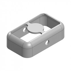
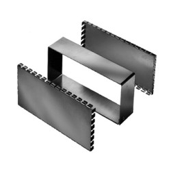
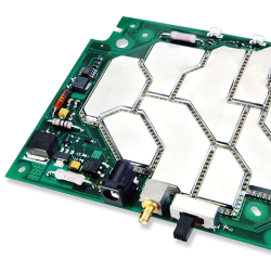
What is a PCB-level shielding enclosure?
PCB shields are simply miniature metal enclosures (often in the form of cans or “caps”) that cover specific parts of an electronic circuit on the PCB. Technically, they act as a Faraday cage, which serves to:
- block external electromagnetic waves before they reach sensitive components (e.g., analog circuits),
- limit emission of interference from the circuit — i.e., contain “noise” at the source.
In practice, PCB-level shielding protects both your electronics and other nearby devices.
Why use PCB-level shielding?
- Protection of sensitive circuits – such as amplifiers, analog converters, RF systems.
- EMC emission reduction – crucial for meeting standards (e.g., CE, FCC).
- Localized noise suppression – more effective than global shielding for high-emission sources.
In many cases, shielding at the PCB stage helps avoid more expensive full-enclosure solutions — meaning lower costs and a simpler design.
Shielding Effectiveness (SE)
To evaluate how well a shield works, we use a parameter called Shielding Effectiveness (SE). It is expressed in decibels (dB) and describes by how many decibels the electromagnetic field strength is reduced thanks to the PCB shield.
SE=20log10(Ewithout/Ewith)
Where:
- Ebez is the field intensity before shielding,
- Ez is the field intensity after applying the shield.
Example: SE = 40 dB means that the shield attenuates the wave by 100 times (in terms of amplitude) or 10,000 times in terms of power.
What affects SE?
Shielding effectiveness depends on many factors:
- the material of the enclosure,
- the thickness of the enclosure,
- the type of EM wave (electric vs. magnetic),
- the presence of holes and gaps,
- signal frequency.
SE is a complex value — which is why the following sections will go deeper into the mechanisms of shield operation and material selection.
How EMI Shielded Enclosures Work
To effectively design EMC shielding, it's not enough to just know the shielding level in decibels. You need to understand how EMI shielding enclosures work physically — that is, what phenomena occur when an electromagnetic wave encounters a barrier. Three fundamental mechanisms come into play: reflection, absorption, and transmission.
Reflection – the first line of defense
When an EM wave hits a conductive material (e.g., copper), a significant portion of the energy is simply reflected. This happens because:
- the electric field cannot penetrate the interior of a perfect conductor (E = 0),
- the magnetic field induces eddy currents, which generate a field that opposes its changes (Lenz's Law).
As a result:
- electrically dominant waves (high impedance) are effectively attenuated by reflection,
- but magnetically dominant waves (low impedance) more easily penetrate thin layers – so reflection alone may not be enough.
Absorption – the second line of defense
The portion of energy that is not reflected enters the shield. Then, the second mechanism kicks in: absorption, or the conversion of EM field energy into heat. It occurs mainly due to:
- eddy currents,
- dielectric losses (if the material is not a perfect conductor).
The degree of absorption depends on several factors:
- the material (e.g., steel absorbs magnetic fields better than copper),
- the layer thickness – in relation to the skin depth,
- signal frequency – the higher it is, the smaller the skin depth, meaning better absorption by a thin shield.
Good to know: For magnetic waves, absorption is more important than reflection, especially at low frequencies.
Transmission – what “leaks through”
Unfortunately, no shield is perfect. Some energy gets through – this is called transmission, or the residual wave that passed through the barrier. The designer's goal is to:
- minimize transmission by properly selecting the material and thickness,
- reduce all gaps and openings through which EMI energy might escape.
When does reflection matter, and when does absorption?
Which shielding mechanism plays a greater role — reflection or absorption — depends on the nature of the electromagnetic wave, i.e., whether the electric or magnetic field dominates. The key parameter that defines this is the wave impedance.
If the wave has a high impedance, close to 377 Ω (which is the impedance of vacuum), it means the electric field is dominant. In such cases, reflection plays the main role in shielding — because electric fields easily reflect off well-conducting surfaces. That’s why materials with high electrical conductivity, like copper or aluminum, are best for attenuating this type of wave.
On the other hand, if the wave has low impedance (much less than 100 Ω), it means the magnetic field dominates. In these cases, reflection is less effective because magnetic fields more easily penetrate thin conductors. This is where the second mechanism — absorption — comes in, converting the wave’s energy inside the material. To make this work, materials with high magnetic permeability are required, such as steel, iron, or in some cases, special ferrite composites.
In practice, many real-world sources of interference emit waves with a mixed character — neither purely electric nor purely magnetic. That’s why most applications use a hybrid approach: combining reflection and absorption mechanisms by selecting materials to ensure shielding is effective across a wide range of frequencies and interference types.
If you're unsure what kind of wave you're dealing with — assume you need both mechanisms. That’s why in practice, composite materials or multilayer shields are often used.
Choosing EMI Shielding Materials – Comparisons and Recommendations
Selecting the right material for EMI shielding is not only about cost and availability, but primarily about its physical properties — electrical conductivity, magnetic permeability, and layer thickness. Every material behaves differently depending on the interference frequency and the dominant field type (electric or magnetic), which directly affects shielding effectiveness.
Copper – the gold standard of shielding
Copper is the most commonly chosen material for EMI shielding – and for good reason. Its very high electrical conductivity makes it excellent at reflecting high-impedance waves, meaning those in which the electric field dominates. As such, it is highly effective in shielding radio circuits, high-frequency signals, and general emissions from PCBs. Copper is also relatively easy to work with and adheres well to the surface of printed circuit boards.
Keep in mind: copper is not ideal for attenuating strong low-frequency magnetic fields – in such cases, a material with higher magnetic permeability is needed.
Steel – when magnetic interference dominates
Steel (specifically – low-carbon soft steel) is excellent at attenuating magnetic fields, especially at low frequencies. This is due to its high magnetic permeability, which enables it to absorb H-field energy within the material. Therefore, steel is well suited for shielding around transformers, motors, power cables, or other sources of magnetic interference.
Its drawbacks include greater weight and lower electrical conductivity than copper, making it less effective at reflecting electric waves – hence it is often used in combination with other materials (e.g., nickel-plated steel or copper-clad steel).
Brass – a compromise choice
Brass, as an alloy of copper and zinc, offers a compromise between cost, conductivity, and mechanical properties. It has slightly lower conductivity than pure copper, but higher corrosion resistance and rigidity. It is suitable for general shielding, especially in mechanically demanding applications – e.g., industrial enclosures or shields formed into complex shapes.
Designing EMC shielding with gaps and openings in mind
In practical applications, an enclosure rarely takes the form of a perfectly solid surface. In real PCB constructions and their housings, there are always gaps, apertures, assembly seams, or ventilation holes. Although often necessary for design reasons, they can significantly reduce shielding effectiveness.
Impact of gaps (seams, openings) on shielding effectiveness
Every gap in the shield is a potential point through which electromagnetic waves can penetrate – both into and out of the protected space. Shielding effectiveness in such cases drops, especially at higher frequencies, where even small gaps can act as slot antennas.
Gaps in the shield may cause:
- Wave leakage – especially at high frequencies, where the wavelength is comparable to or smaller than the dimensions of the opening.
- Resonance – the opening may begin to resonate at certain wavelengths, increasing signal transmission.
Cutoff frequency – what it is and how to calculate it
The concept of cutoff frequency refers to the maximum frequency at which a given opening or gap can still effectively attenuate EM waves. Above this frequency, shielding becomes ineffective.
For a rectangular opening in a shield, the approximate cutoff frequency can be estimated with the formula:
f_c ≈ 15 / d
Where:
- f_c – cutoff frequency in GHz
- d – the longest dimension of the opening in centimeters
For example: an opening 2 cm long will allow waves above approx. 7.5 GHz to pass through.
Best practices: maximum hole size vs. wavelength
To prevent openings from degrading shielding, their dimensions should be much smaller than the wavelength, ideally less than λ/20. For a frequency of 1 GHz (wavelength approx. 30 cm), the maximum hole diameter should be below 1.5 cm.
Best design practices include:
- avoiding long gaps,
- using contact gaskets and grounding points (stitching vias),
- shielding gaps with conductive materials (e.g., EMI gaskets),
- locally sealing key signal I/O points.
Practical PCB design tips
EMI shielding should not be treated as an afterthought in the final design stage. On the contrary – the best results are achieved when electromagnetic interference protection is an integral part of the PCB design process from the very beginning.
Why plan shielding early in the design process?
Designing a PCB without considering EMI often leads to a "reactive" approach – we first design the circuit, and only after testing do we add shielding where problems arise. Unfortunately, such actions are costly, often require redesign, and rarely provide full effectiveness.
Planning shielding in advance allows you to:
- optimize signal routing and component placement,
- select an appropriate layer stack-up (e.g., ground plane as a shield),
- minimize current loops and coupling between circuits,
- account for physical space for metal covers or EMC foil shields,
- reduce costly corrections at later stages.
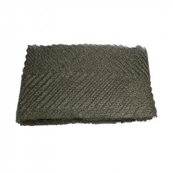
Off-the-shelf solutions from manufacturers
There are many ready-made “off-the-shelf” solutions available on the market that simplify the implementation of EMI shielding without needing to design everything from scratch. These include:
- soldered shields (shield cans) – available in various dimensions, with optional SMT solderable frames,
- EMI gaskets – conductive elements mounted along shield or enclosure edges, ensuring electrical contact,
- shielding foils and tapes – for temporary or flexible shielding of selected areas,
- composite materials – for shielding plastic enclosures.
The specific solution should be selected based on PCB space, type of EMI threats, ease of assembly, and production costs.
Cost vs. effectiveness – how to optimize your design
EMI shielding design is about finding a balance between cost and effectiveness. Excessive shielding (e.g., full metal cages over the entire board) increases weight, production costs, and assembly complexity – often without proportional benefit.
On the other hand, overly frugal approaches (e.g., relying only on filters or a ground layer) may not suffice in high-interference environments.
Optimization includes:
- applying shielding only where justified (e.g., around EMI sources or victims),
- using existing components (e.g., the enclosure as part of the shield),
- selecting effective materials (copper where reflection is key; steel when absorption is important),
- using inexpensive, mass-produced shielding components from reputable suppliers.
Conclusion – key takeaways for electronics designers
Electromagnetic interference (EMI) is a significant challenge in modern electronics design. Its presence can not only degrade device performance but may even prevent proper operation. Therefore, shielding at the PCB level is not just a wise decision but a necessary design element.
Key conclusions and best practices:
- EMI must be addressed already at the design stage. Waiting until final testing to implement shielding is unwise – planning protection at the PCB level delivers the greatest benefits and minimizes cost.
- Understanding electromagnetic wave characteristics (E and H components, wave impedance) enables informed selection of shielding methods and materials.
- Shielding effectiveness depends on the mechanism: reflection, absorption, and wave transmission. It's important to understand when reflection dominates (electric fields) and when absorption dominates (magnetic fields), to choose materials appropriately (e.g., copper, steel, brass).
- EMI shield design must consider details such as gaps, seams, and holes. Their size and placement must be matched to the wavelength to avoid compromising shielding effectiveness.
- Choosing materials and off-the-shelf solutions requires a balance between cost and efficiency. Full metal enclosures are often unnecessary – smart PCB-level shielding and thoughtful component placement usually suffice.
- Ready-made components and technologies (e.g., soldered shields, EMC foils, gaskets) simplify implementation and accelerate production.
Ultimately, effective PCB-level shielding often proves more efficient and economical than trying to fix EMI issues at the enclosure level.
Implementing consistent, well-considered EMI protection practices enables not only compliance with standards and certifications but, most importantly, ensures stable and reliable device operation in harsh electromagnetic environments.
Sources:
1. Paul, C. R. – Introduction to Electromagnetic Compatibility. A comprehensive introduction to EMC concepts, ideal for electronics designers.
2. Ott, H. W. – Electromagnetic Compatibility Engineering. A practical guide to designing and testing EMI-resistant systems.
3. Pozar, D. M. – Microwave Engineering. Covers electromagnetic wave propagation fundamentals and impedance, helpful for understanding EMI physics.
4. EMC standards and guidelines (e.g., CISPR, EN 55032). Official documents regulating emissions and immunity requirements for devices.
5. Technical materials from shielding material manufacturers (e.g., 3M, Laird, TC Shielding, TEMAS). Detailed data on EMI shielding materials and application examples.
Related products


Related posts
Thermally conductive materials in power storages
Technological development caused a need in electric engineering to search for new solutions in heat conduction.
Read more
Measuring power and energy in electric circuits
Power meters and network parameter analyzers are intended for identifying anomalies of power supply in single-phase...
Read more
Wentylatory przemysłowe - rodzaje, właściwości
W zależności od obiektu, charakteru stanowisk pracowniczych, oraz szeregu indywidualnych czynników otoczenia w...
Read more
Leave a comment