Thermal Clad is a versatile substrate allowing circuit boards to be configured for shapes, bends and multiple thicknesses. In this motor control application, the dielectric has been selectively removed and the metal formed with three-dimensional features.
Additional Thermal Clad benefits: • Increased power density • Extend the life of dies • Improved product thermal and mechanical performance • Better use of surface mount technology
Anatomy of a Thermal Clad Board: 1. Base layer Copper 0,51 - 4,83 mm oa Aluminium 0,51 - 3,18 mm. 2. Dielectric layer – HPL, HT, LM, MP. 3. Circuit layer – 35 um – 350 um.
Parameters:
Type
Thickness (10-3in/10-6m)
Impedance (oC/W)
Conductivity (W/m-k)
Operating (VAC)
Breakdown (kVAC)
HT-04503
3/75
0.45
2.2
120
6.0
HT-07006
6/150
0.70
2.2
960
11.0
LTI-04503
3/75
0.45
2.2
120
6.5
LTI-06005
5/125
0.60
2.2
480
9.5
MP-06503
3/75
0.65
1.3
120
8.5
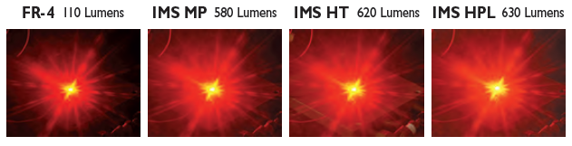
Light output of the same LED die on different circuit board materials at a maintained die temperature of 80ºC.
Thermal Clad is a versatile substrate allowing circuit boards to be configured for shapes, bends and multiple thicknesses. In this motor control application, the dielectric has been selectively removed and the metal formed with three-dimensional features.
Additional Thermal Clad benefits: • Increased power density • Extend the life of dies • Improved product thermal and mechanical performance • Better use of surface mount technology
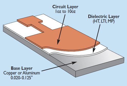
Anatomy of a Thermal Clad Board: 1. Base layer Copper 0,51 - 4,83 mm oa Aluminium 0,51 - 3,18 mm. 2. Dielectric layer – HPL, HT, LM, MP. 3. Circuit layer – 35 um – 350 um.
Parameters:
Type
Thickness (10-3in/10-6m)
Impedance (oC/W)
Conductivity (W/m-k)
Operating (VAC)
Breakdown (kVAC)
HT-04503
3/75
0.45
2.2
120
6.0
HT-07006
6/150
0.70
2.2
960
11.0
LTI-04503
3/75
0.45
2.2
120
6.5
LTI-06005
5/125
0.60
2.2
480
9.5
MP-06503
3/75
0.65
1.3
120
8.5
Light output of the same LED die on different circuit board materials at a maintained die temperature of 80ºC.