shopping_cart
Karte
0,00 PLN
0
Zwischenablage
Sie müssen eingeloggt sein
-
-
-
Category
-
Halbleiter
- Dioden
- Thyristoren
- Elektroisolierte Module
- Brückengleichrichter
-
Transistoren
- Transistoren | GeneSiC
- SiC-MOSFET-Module | Mitsubishi
- SiC-MOSFET-Module | STARPOWER
- ABB SiC-MOSFET-Module
- IGBT-Module | MITSUBISHI
- Transistormodule | MITSUBISHI
- MOSFET-Module von MITSUBISHI
- Transistormodule | ABB
- IGBT-Module | POWEREX
- IGBT-Module | INFINEON (EUPEC)
- Halbleiterkomponente aus Siziliumkarbid
- Przejdź do podkategorii
- Treiber
- Leistungsblöcke
- Przejdź do podkategorii
- Strom- und Spannungswandler von LEM
-
Passive Elemente (Kondensatoren, Widerstände, Sicherungen, Filter)
- Widerstände
-
Sicherungen
- Miniatursicherungen für elektronische Schaltungen der Serien ABC und AGC
- Schnelle Röhrensicherungen
- Zeitverzögerungssicherungen mit GL / GG- und AM-Eigenschaften
- Ultraschnelle Sicherungseinsätze
- Britische und amerikanische schnelle Sicherungen
- Schnelle europäische Sicherungen
- Traktionssicherungen
- Hochspannungs-Sicherungseinsätze
- Przejdź do podkategorii
-
Kondensatoren
- Kondensatoren für Motoren
- Elektrolytkondensator
- Island Filmkondensatoren
- Leistungskondensatoren
- Kondensatoren für Gleichstromkreise
- Kondensatoren zur Leistungskompensation
- Hochspannungskondensatoren
- Induktionsheizkondensatoren
- Impulskondensatoren
- DC LINK-Kondensatoren
- Kondensatoren für AC / DC-Schaltungen
- Przejdź do podkategorii
- Entstörungsfilter
- Superkondensatoren
- Überspannungsschutz
- TEMPEST-Strahlungserkennungsfilter
- Überspannungsableiter
- Przejdź do podkategorii
-
Relais und Schütze
- Theorie der Relais und Schütze
- Dreiphasen-Halbleiterrelais AC
- Halbleiterrelais DC
- Regler, Steuerungen und Zubehör
- Sanftstarter und Schaltschütze
- Elektromechanische Relais
- Schütze
- Drehschalter
-
Einphasen-Halbleiterrelais AC
- Einphasen-Wechselstrom-Halbleiterrelais, Serie 1 | D2425 | D2450
- Einphasige AC-Halbleiterrelais der Serien CWA und CWD
- Einphasen-Wechselstrom-Halbleiterrelais der Serien CMRA und CMRD
- Einphasen-Wechselstrom-Halbleiterrelais, PS-Serie
- Doppel- und Vierfach-Wechselstrom-Halbleiterrelais, Serie D24 D, TD24 Q, H12D48 D.
- 1-phasige Festkörperrelais, gn-Serie
- Einphasige Wechselstrom-Halbleiterrelais, Serie ckr
- Einphasen-Wechselstromrelais der ERDA- UND ERAA-SERIE für die DIN-Schiene
- Einphasige Wechselstromrelais für 150A Strom
- Doppelte Halbleiterrelais mit integriertem Kühlkörper für eine DIN-Schiene
- Przejdź do podkategorii
- Einphasen-Halbleiterrelais AC für Leiterplatten
- Interface-Relais
- Przejdź do podkategorii
- Induktive Komponente
- Radiatoren, Varistoren, Thermoschütze
- Ventilatoren
- Klimaanlagen, Ausrüstung für Schaltschränke, Industriekühler
-
Batterien, Ladegeräte, Pufferstromversorgungen und Wechselrichter
- Batterien, Ladegeräte - theoretische Beschreibung
- Lithium-Ionen-Batterien. Kundenspezifische Batterien. Batteriemanagementsystem (BMS)
- Batterien
- Ladegeräte und Zubehör
- USV-Notstromversorgung und Pufferstromversorgung
- Konverter und Zubehör für die Photovoltaik
- Energiespeicher
- Brennstoffzellen
- Lithium-Ionen-Batterien
- Przejdź do podkategorii
-
Automation
- Spiralift Hebebühnen
- Futaba Drohnenteile
- Grenzschalter, Microschalter
- Sensoren, Wandler
-
Pyrometer
- Infrarot-Temperatursensor, kabellos, wasserdicht, IR-TE-Serie
- Infrarot-Temperatursensor, kabellos, IR-TA-Serie
- Infrarot-Temperatursensor, kabellos, IR-H-Serie
- Ein schnelles stationäres Pyrometer in einem sehr kleinen IR-BA-Gehäuse
- Lichtleiter-Temperatursensoren, IR-FA-Serie
- Das stationäre Pyrometer der IR-BZ-Serie
- Przejdź do podkategorii
- Zähler, Zeitrelais, Einbaumessgeräte
- Industrielle Schutzausrüstung
- Licht- und Signalentechnik
- Infrarot-Kamera
- LED-Anzeigen
- Taster, Schalter und Zubehör
- Przejdź do podkategorii
-
Adern, Litzen, Schutzhüllen, Flexible Verbingungen
- Drähte
- Kabeleinführungen und Kupplungen
- Litzen
-
Kabel für spezielle Anwendungen
- Verlängerungskabel und Kompensations
- Kabel für Thermoelemente
- Die Verbindungsdrähte zu czyjnków PT
- Mehradrige Kabel Temp. -60 ° C bis + 1400 ° C
- SILICOUL Mittelspannungskabeln
- Zündkabel
- Heizleitungen
- Einadriges Temp. -60 ° C bis + 450 ° C
- Zugbegleiter
- Heizleitungen im Ex
- Kabel für die Verteidigungsindustrie
- Przejdź do podkategorii
- Schläuche
-
Geflochtene Kabel
- Zöpfe flach
- Zöpfen Runde
- Sehr flexible Geflecht - flach
- Sehr flexible Geflecht - Rund
- Kupfergeflecht zylindrischen
- Kupfergeflechtschirm und zylindrischer
- Flexible Massebänder
- PVC-isolierte Kupferlitzen - Temperatur 85 ° C
- Flach geflochtene Aluminium
- Connection Kit - Zöpfe und Röhren
- Stahlgeflechte
- Przejdź do podkategorii
- Leitungen und Sonstiges für Traktion
- Crimpverbinder
- Flexible isolierte Kupferschienen
- Mehrschichte flexible Kupferschienen
- Kabelrohre, Kabelkanäle und Kabelführung
- Przejdź do podkategorii
- Zobacz wszystkie kategorie
-
Halbleiter
-
-


Moderne Methoden, die bei der Entwicklung von Unterhaltungselektronik eingesetzt werden

Imagine for a moment that you are testing a completely new car: you sit in one of the ergonomic seats, start the engine, and to complete the experience, you want to listen to music. However, when you turn on the radio, you suddenly notice interesting side effects. For example, the passenger cabin light turns on. Or the radio starts to squeal and whine. These are relatively harmless phenomena. However, much more serious problems can occur, which may even endanger driving safety or limit the functionality of the car. High-frequency interference is very troublesome in modern electric cars, hybrid vehicles, or complex electronic systems that ensure driver safety and comfort.

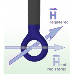
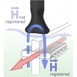
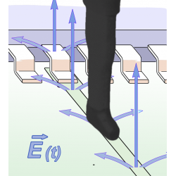
Fig. 1 The element radiates to the driver's seat metal structure via a near electric field. The driver’s seat, thus excited, emits waves to the vehicle antenna, interfering with the radio signal reception.
Sources of Emission and Limitations of Traditional EMC Measurements
Usually, it is not the entire electronic component, but an individual device that is responsible for emissions. A device such as a quartz resonator or microcontroller generates local electromagnetic fields that induce voltages in housings or structural parts. These parts are thus stimulated to oscillate and, as a result, emit radiation. A software developer will certainly check their components for emissions by performing component measurements in an EMC test chamber during development. However, these measurements generally measure emissions from the tested device as a whole. The measurement methods used in such tests are not able to sufficiently assess the near fields of the tested device. During conventional measurements, the designer cannot directly interact with the tested device, measure individual sections of the component in detail, or take any action to locate the source of emissions. The tested device is removed from the EMC chamber, placed in packaging, and returned to its workplace. Another problem with these component measurement methods is that the component is tested outside the actual vehicle environment, and emission frequencies may not be measured because other nearby structural parts are not stimulated to oscillate.
Upon returning to their workplace, the programmer can only compare frequency images from the component test with those obtained from other development processes and formulate hypotheses about the causes of problems. Then they modify the tested device based on these hypotheses. Only further test measurements in the EMC chamber show whether the change was correct and effective. The measurement setup must be repeated for new component measurements. However, in most cases, the component, especially the wiring harness, cannot be restored to exactly the same position. This causes measurement deviations. Frequency response characteristics measured at different stages of component development cannot be compared immediately and flexibly. The designer must place individual protocols side by side and compare them step by step. This approach to EMC component development is time-consuming, complex, and unsatisfactory for the designer – requiring significant effort and resulting in high costs.
The Need for More Effective Detection of Interference Sources
In this case, more effective detection of emission sources in complex electronic systems is necessary during development. The engineer must be able to measure as many disturbances as possible, systematically identify RF sources, flexibly make modifications, and carry out tests in their workplace to save time and costs.
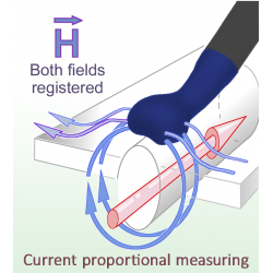
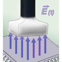
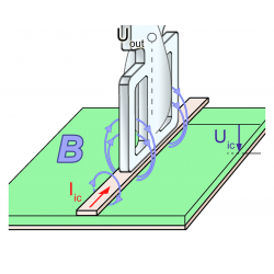
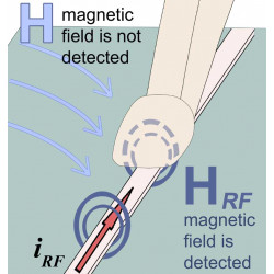
Now let's look at how a component can become a source of emissions. The electronic circuit or printed conductor itself usually does not emit any waves. However, individual devices can generate near RF fields that surround, for example, connected cables. They induce voltage in them, causing emission. Due to electrical or magnetic coupling (i.e., in the near field), the entire metal system, including the component and connected cables, as well as nearby metal parts such as housings, shielding plates, etc., undergoes self-excitation. (Fig. 2).
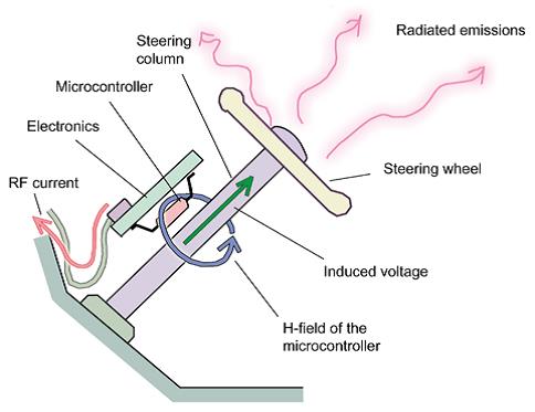
Fig. 2: A microcontroller placed on a component emits a magnetic field. It surrounds the steering column, inducing a voltage. This voltage stimulates the steering column to emit radiation, which can interfere with sensitive components near the driver’s seat.
Modern Methods of Emission Measurement at the Engineer’s Workplace
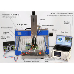
The entire metal system acts as an antenna when excited by electronics. The RF excitation current flowing from the electronics to the antenna (cables and metal parts) can therefore be considered an approximate measure of emissions from the tested device. We will now describe a measurement setup that meets our requirements for effective component development in terms of emissions. Emissions are measured under conventional measurement conditions, for example using an antenna. The device under test must be modified if one or more frequencies of the development sample exceed the limit values defined in the relevant standard. The values obtained from this measurement are used as a reference point for subsequent comparative measurements. (Fig. 3)
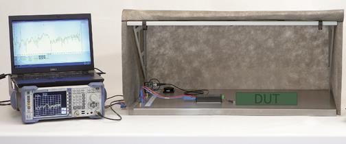
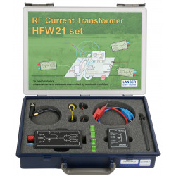
Fig. 3: ESA1 system with ChipScan-ESA software and spectrum analyzer.
Near Field Measurement and the Use of a Shielding Tent
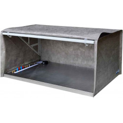
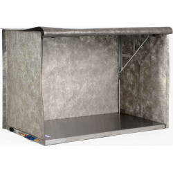
During emission measurement from electronic circuits at the programmer’s workplace, it is important to define a measurement setup that simulates the component environment in the passenger cabin as accurately as possible. A closed measurement configuration is set up at the workplace to measure all reasonable RF currents of the tested device. If relevant frequencies fall within a range subject to strong external interference, such as radio frequencies, a shielding tent is used to protect the measurement setup from these disturbances. The shielding tent has a surface area of 50×90 cm and attenuation of over 40 dB in the frequency range from approximately 80 to 650 MHz. The front of the shielding tent can be folded up and down. The entire shielding tent can be widely opened to facilitate modification of the tested device. Power supply cables, such as electrical power and measurement signal cables, are routed outside through filtered feedthroughs in the ground plane. This also creates a stable grounding for the tested device and measurement equipment parts.
How are measurements conducted at the programmer’s workplace? In the first stage, comparative measurements are performed using RF current probes in the closed shielding tent and documented. The results of these measurements are compared with component measurement results to confirm the correctness of the measurement setup. Of course, the measurement results will not match exactly. However, it is important that the relevant frequencies from the component measurement are also present in the frequency image of the selected measurement setup.
Identification and Elimination of RF Radiation Sources
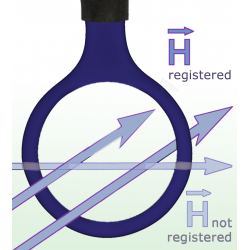
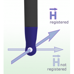
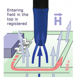
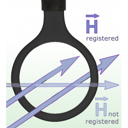
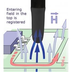
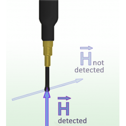
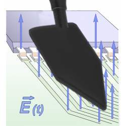
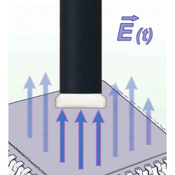
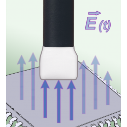
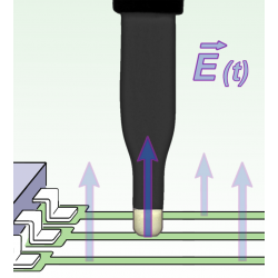
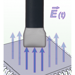
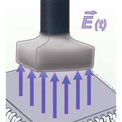
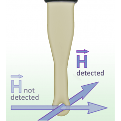
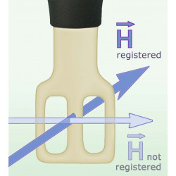
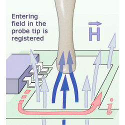
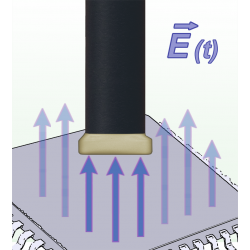
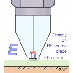
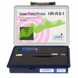
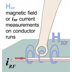
In the next step, electric and magnetic field probes are used to scan integrated circuits, line connections, plug connectors, etc. Precise frequency and near-field orientation analysis often allows the programmer to recognize correlations between fields and excitation currents. To measure near fields using probes, the front of the shielding tent must be opened. Naturally, the shielding effect is then much lower than in the closed tent. However, the near fields of the tested device are usually much stronger than fields coupled from the environment, allowing measurements to be successfully carried out. Field intensity at a given frequency and in a given frequency range (Fig. 4 and Fig. 5).
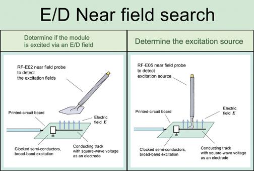
Fig. 4
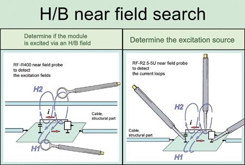
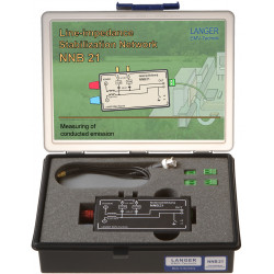
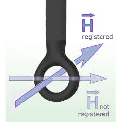
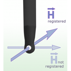
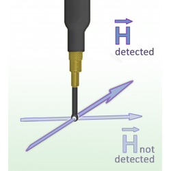
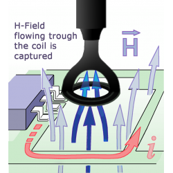
Fig. 5: Use of electric and magnetic field probes to measure near fields on components and their devices.
Possible sources of radio radiation include:
- electric fields above devices such as processors,
- electric fields on switched lines and bus systems,
- magnetic fields on switched data and clock lines,
- magnetic fields in power supplies.
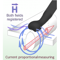
After identifying RF interference sources, the board can be modified on-site by soldering components, using shielding measures, or changing wire routing. Further measurements using an RF current probe in the closed shielding tent immediately show whether the measures are effective. RF current probes and near-field probes can be used alternately for measurements in subsequent tests. The element can be continuously modified until the RF current flowing through the power line from the RF current probe is minimized. Measured frequency response characteristics can be documented using a PC and customized software. This software allows programmers to record, color, annotate, calculate, and visualize any number of spectrum analyzer traces and enables flexible, easy, and fast comparison of different stages of the measurement process. Programmers can simply export images and data from the software for documentation and statistical analysis. (Fig. 6)
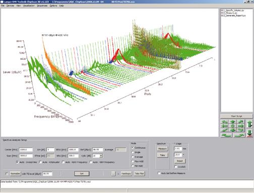
Fig. 6: Large amounts of various data provided by the spectrum analyzer can be conveniently measured and compared using ChipScan-ESA software.
Testing Connectors and Integrated Circuits for EMC
A closer look at component electromagnetic compatibility issues shows that plug connectors, especially those used in high-voltage hybrid car systems, are unique. They are subject to high EMC requirements. Testing such connectors in a component prototype is actually too late, as the designer cannot improve the connector. Therefore, the designer should test individual connectors for their EMC characteristics early in the design process or rely on connectors with known EMC parameters that are deemed sufficient for the given component.

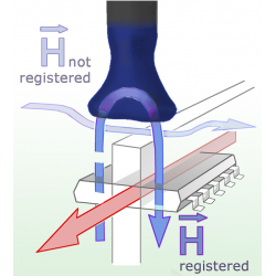
Fig. 7: The designer was able to identify the emission source in Fig. 1 by detecting near fields. In this case, radio reception interference could be prevented by moving the emission-causing element to a location in the car where no parts could be stimulated to oscillate nearby.
In addition to devices with one or two cable connections, complex devices can also be tested. At the start of the test, various effects caused by different RF sources in the tested device overlap and lead to reinforcement or partial cancellation of RF fields at specific frequencies. Therefore, to conduct an effective root cause analysis, especially for complex devices composed of multiple PCBs, it is important that the device is disassembled into manageable parts and individual PCBs are examined separately. The device under test shown in Fig. 8 has several potential emission sources. In this example, the study is limited to the component interface module.
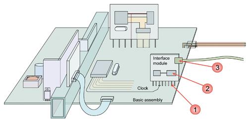
Fig. 8: Possible emission sources of the interface module in a complex system.
We can imagine three RF sources:
1. connector between the base assembly and the interface module
2. electronics (PHY with microprocessor) in the interface module
3. interface cable connector
These three RF sources will now be discussed in order. This requires a measurement setup that suppresses other RF sources and the base assembly RF sources as much as possible.
1. Connector between the base assembly and the interface module (Fig. 9)
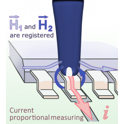
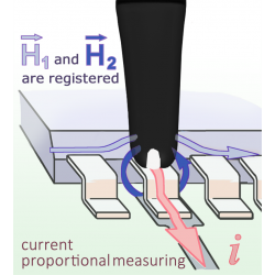
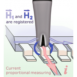
The base assembly and interface module are connected via data and control lines. These lines are well shielded on the PCB in the base assembly and interface module areas, as they are embedded in grounded planes. However, in the connector area, they pass freely through open space. Signal currents in the lines generate RF magnetic fields that spread inside and around the connector. They generate induced voltages in the connector ground pins. As a result, a voltage difference occurs between the base assembly and the interface module. This causes RF current to flow to the cable via the interface PCB, which in turn excites the cable and thus its emissions. The COM port of the current probe is connected close to the GND of the interface module to measure the current driven by the induced voltage. The effect of modifications such as filters on signal lines or pin reassignment can be measured directly.
Fig. 9: First measurement stage using ESA1 – detection of emission sources at the connector between the base assembly and interface module
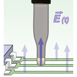
2. Electronic circuits (PHY with microprocessor) on the interface module (Fig. 10).
The integrated circuits of the interface module generate currents that flow to the GND system, inducing voltage. This voltage, in turn, drives current from the base assembly to the connected interface cable, which excites the cable to emit. The base assembly remains connected to the ground plane during measurement. The contribution of the connector to emissions between the ground plane and the interface module is reduced by several large GND connections. Voltage induced by the currents of the ICs can be measured using a current probe at the top of the assembly. Modifications made directly on the interface module can thus be assessed.
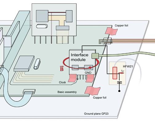
Fig. 10: Second measurement stage using ESA1 – detecting emission sources in electronics
3. Interface cable connector (Fig. 11)
The interface connector is another RF source in this complex component. During data transfer, the interface driver passes current through the connector. This current induces voltage along the connector housing, stimulating emissions from the interface cable. The current probe is connected to the interface cable to perform the measurement. Note that during this measurement, the voltage is applied as described in point 2 above. This voltage can be shorted by attaching a piece of copper foil to the interface PCB.
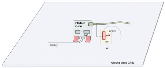
Fig. 11: Third measurement stage using ESA1 – detecting emission sources at the interface cable connector.
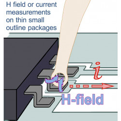
The integrated circuit is another electronic element that is important for the component designer. The characteristics of ICs used in the electronic system have a large impact on the EMC characteristics of the entire component. Microcontroller and chipset structures are becoming smaller. Therefore, IC sensitivity can now be up to ten times higher than their previous models. The behavior of ICs and their package types regarding immunity and emissions is a key aspect that the designer must consider when selecting devices for a component. Therefore, it is important to choose the right IC and use it according to the relevant EMC requirements during the component development planning stage. EMC compliance measurements according to BISS/IEC standards should be carried out on ICs with respect to EMC parameters as a standard procedure. However, these measurements are not sufficient to ensure the IC will perform properly in practice. Furthermore, ICs should be tested using practical and universal EMC parameters, such as ESD. Impulses occurring in ICs during ESD and device impulse tests can be simulated in IC immunity tests. Special IC measurement and testing technology should allow the designer to perform immunity tests independently of the device or component. (Fig. 12)
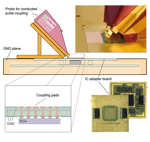
Fig. 12: Shows the test setup for direct coupling of disturbances to the LFBGA package. The IC is mounted on a special IC adapter board. Disturbances can be applied directly to BGA balls using P200/P300 series probes. External IC wiring follows the manufacturer's specification. Additionally, filter components are used in power and signal lines to prevent discharge of the disturbance pulse, ensuring specific conditions.
During IC emission analysis, the designer must thoroughly examine the physical component process. For example, if a fast high-frequency current and voltage circuit is placed in an unfavorable location in the device, it may interfere with the operation of the component itself or other components or devices via coupling paths through the component.
Conclusions: Effective EMC Planning in Component Development
1. Test results help achieve three objectives:
2. Improving IC to avoid problems during later use
3. Practical parameters and conditions for interference-free use of the IC in components
4. Selecting an IC suitable for the user application based on the IC's EMC parameters. This gives the electronics programmer access to procedures and information that help plan EMC for a complex component in advance and measure and modify it directly in their workplace during the development process. Development becomes more efficient and less time-consuming. Fewer component tests in the EMC chamber will be required. This reduces long waiting times when the EMC chamber is needed. Consequently, component development accelerates, saving resources, time, and costs.
Ähnliche Produkte


Ähnliche Beiträge
Wärmeleitende Materialien in Energiespeichern
In der Elektrotechnik hat der technologische Fortschritt dazu geführt, dass neue Lösungen zur Wärmeableitung benötigt...
Read more
Messung von Leistung und Energie in elektrischen Stromkreisen
Leistungsmesser und Netzparameteranalysatoren sind Geräte, die zur Erkennung von Leistungsanomalien in Einphasen-...
Read more
Industrielüfter – Typen, Eigenschaften
Je nach Anlage, Art der Arbeitsplätze und einer Reihe individueller Umweltfaktoren werden in der Industrie...
Read more
Hinterlassen Sie einen Kommentar